![]()
![]()
![]()
Use LEFT and RIGHT arrow keys to navigate between flashcards;
Use UP and DOWN arrow keys to flip the card;
H to show hint;
A reads text to speech;
73 Cards in this Set
- Front
- Back
|
Subsurface imperfections in board material
|
such as delamination, blistering, and foreign inclusions.
|
|
|
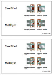
Subsurface imperfections to multilayer printed boards
|
such as voids, delamination, blistering, cracks, ground plane clearance and layer to layer spacing.
|
|
|
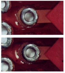
Plated-through hole anomalies
|
including size, annular ring, nailheading, plating thickness, plating voids, nodules, cracks, resin smear, inadequate or excessive etchback, wicking, inner layer (post) separation, and solder resist thickness.
|
|
|
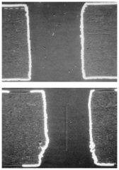
Internal conductor anomalies
|
such as over or under etch, conductor cracks and voids, uneven or inadequate oxide treatment, and foil thickness.
|
|
|
Visual observations
|
made on cross-sections only.
|
|
|
Registration of conductors
|
is typically determined with respect to plated-through hole lands.
|
|
|
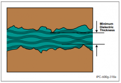
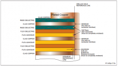
Minimum dielectric thickness
|
is the maximum material condition used for the electrical voltage dielectric strength requirements.
|
|
|
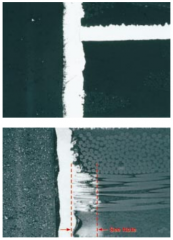
Smear removal
|
is defined as the removal of resins debris which results from the formation of the hole.
|
|
|
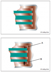
Metal planes
|
are used for mechanical reinforcement and/or electromagnetic shielding for printed boards
|
|
|
Minimum dielectric thickness
|
is the maximum material condition used for the electrical voltage dielectric strength requirements.
|
|
|
Resin recession in a plated-through hole
|
is generally defined as a separation between the plated barrel of the hole and the dielectric material on the hole wall.
|
|
|
Outgrowth
|
The increase in conductor width at one side of the conductor, caused by plating buildup over that delineated by theproduction master.
|
|
|
Undercut
|
The distance on one edge of the conductor measured parallel to the board surface from the outer edge of the conductor, including etch resists, to the maximum point indentation to the copper conductor.
|
|
|
Overhang
|
The sum of the outgrowth and undercut
|
|
|
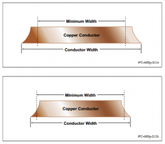
Design width of conductor
|
The width of a conductor as delineated or noted on the procurement documentation
|
|
|
Production Master
|
A 1 to 1 scale pattern which is used to produce one or more printed boards within the accuracy specifiedon the Procurement Documentation.
|
|
|
Etch Factor
|
The ratio of the depth of etch to the amount of lateral etch.
|
|
|
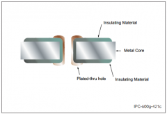
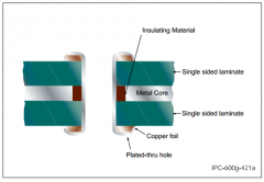
Laminated Type Metal Core Board
|
Single conductive layer on both sides and insulated from themetal core substrate. Conductive material to be copper foiland electrodeposited copper.
|
|
|
The following general rules minimize surface contaminants when handling printed boards:
|
1. Work stations should be kept clean and neat.
2. There should be no eating, drinking or use of tobacco products at the work station or other activities that are likely to causecontamination of the board surfaces. 3. Hand creams and lotions containing silicone should not be used since they could result in solderability and other processingproblems. Specially formulated lotions are available. 4. Handling of boards by their edges is desirable.5. Lint free cotton or disposable plastic gloves should be used when handling bare boards. Gloves should be changed frequentlyas dirty gloves can cause contamination problems.6. Unless special racks are provided, stacking boards without interleaving protection should be avoided. |
|
|
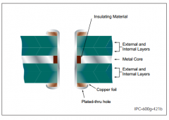
Laminated Type Metal Core Multilayer Board |
More than one conductive layer on one or both sides andinsulated from the metal core substrate. Conductive materialto be copper foil and electrodeposited copper. |
|
|
Annular Ring - Internal Layers
|
|
|
|
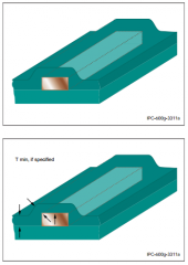
"Clearance Hole, Unsupported, to Power or Ground Planes"
|
|
|
|
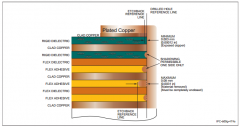
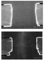
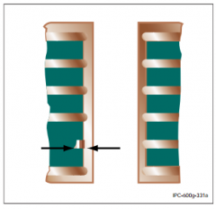
CONDUCTIVE PATTERNS - GENERAL - Print and Etch
|
|
|
|
Core Bond to Plated-Through Hole Wall
|
|
|
|
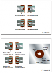
"Cracks in Insulation Material Fill, Laminated Type"
|
|
|
|
DIELECTRIC MATERIAL - Delamination or Blister
|
|
|
|
"DIELECTRIC MATERIAL - Dielectric Material, Clearance, Metal Plane for Supported Holes"
|
|
|
|
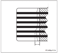
DIELECTRIC MATERIAL - Etchback
|
|
|
|
DIELECTRIC MATERIAL - Layer-to-Layer Spacing
|
|
|
|
DIELECTRIC MATERIAL - Negative Etchback
|
|
|
|
DIELECTRIC MATERIAL - Resin Recession
|
|
|
|
DIELECTRIC MATERIAL - Smear Removal
|
|
|
|
FLEXIBLE AND RIGID-FLEX PRINTED WIRING - Access Hole Registration for Coverlayer and Stiffeners
|
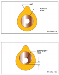
|
|
|
FLEXIBLE AND RIGID-FLEX PRINTED WIRING - Adhesive Squeeze-Out - Foil Surface
|
|
|
|
FLEXIBLE AND RIGID-FLEX PRINTED WIRING - Adhesive Squeeze-Out - Land Area
|
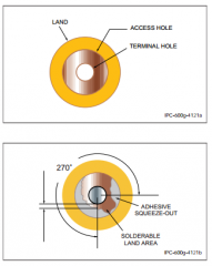
|
|
|
FLEXIBLE AND RIGID-FLEX PRINTED WIRING - Coverlayer Coverage - Coverfilm Separations
|
|
|
|
FLEXIBLE AND RIGID-FLEX PRINTED WIRING - Etchback (Type 3 and Type 4 Only)
|
|
|
|
FLEXIBLE AND RIGID-FLEX PRINTED WIRING - Laminate Integrity - Flexible Printed Wiring
|
|
|
|
FLEXIBLE AND RIGID-FLEX PRINTED WIRING - Laminate Integrity - Rigid-Flex Printed Wiring
|
|
|
|
FLEXIBLE AND RIGID-FLEX PRINTED WIRING - Laminate Integrity
|
|
|
|
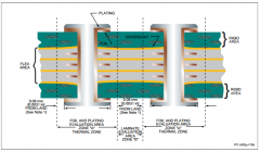
FLEXIBLE AND RIGID-FLEX PRINTED WIRING - Plating Defects
|
|
|
|
FLEXIBLE AND RIGID-FLEX PRINTED WIRING - Smear Removal (Type 3 and 4 Only)
|
|
|
|
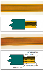
FLEXIBLE AND RIGID-FLEX PRINTED WIRING - Solder Wicking_Plating Migration Under Coverlayer
|
|
|
|
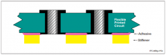
FLEXIBLE AND RIGID-FLEX PRINTED WIRING - Stiffener Bonding
|
|
|
|
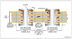
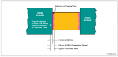
"FLEXIBLE AND RIGID-FLEX PRINTED WIRING - Transition Zone, Rigid Area to Flexible Area"
|
|
|
|
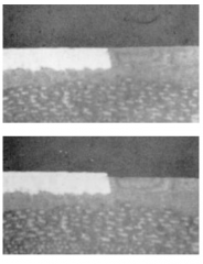
FLEXIBLE AND RIGID-FLEX PRINTED WIRING - Trimmed Edges_Edge Delamination
|
|
|
|
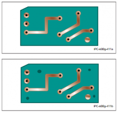
FLUSH PRINTED BOARDS - Flushness of Surface Conductor
|
|
|
|
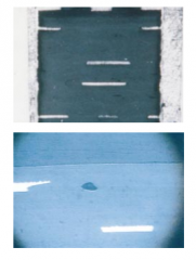
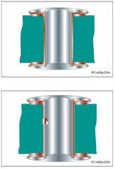
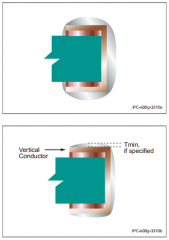
Innerlayer Separation - Horizontal (Transverse) Microsection
|
|
|
|
Innerlayer Separation - Vertical (Axial) Microsection
|
|
|
|
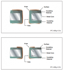
Insulated-Metal-Substrate Metal Core Board
|
|
|
|
"Insulation Material Fill, Laminated Type Metal Core"
|
|
|
|
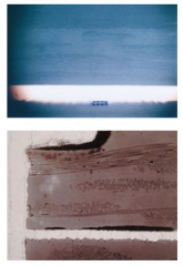
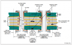
Laminate Voids (Outside Thermal Zone)
|
|
|
|
Laminated Type Metal Core Board
|
|
|
|
Laminated Type Metal Core Multilayer Board
|
|
|
|
"METAL CORE PRINTED BOARDS - Insulation Thickness, Insulated Metal Substrate"
|
|
|
|
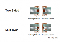
METAL CORE PRINTED BOARDS - Spacing Laminated Type
|
|
|
|
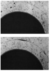
PLATED-THROUGH HOLES - DRILLED - Burrs
|

|
|
|
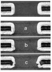
PLATED-THROUGH HOLES - DRILLED - Nailheading
|
|
|
|
PLATED-THROUGH HOLES - GENERAL - Copper Plating Thickness - Hole Wall
|
|
|
|
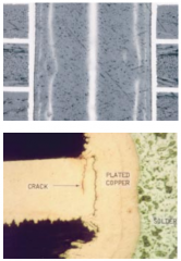
PLATED-THROUGH HOLES - GENERAL - Foil Crack (External Foil)
|
|
|
|
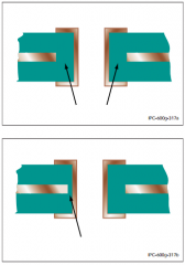
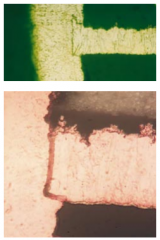
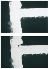
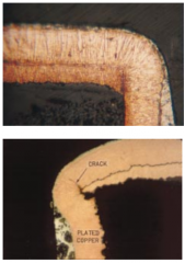
PLATED-THROUGH HOLES - GENERAL - Plating Crack - (Corner) ``F'' Crack
|
|
|
|
PLATED-THROUGH HOLES - GENERAL - Plating Nodules
|
|
|
|
PLATED-THROUGH HOLES - GENERAL - Plating Voids
|
|
|
|
PLATED-THROUGH HOLES - GENERAL - Solder Coating Thickness (Only When Specified)
|
|
|
|
PLATED-THROUGH HOLES - GENERAL - Solder Resist Thickness
|
|
|
|
"PLATED-THROUGH HOLES - GENERAL - Wicking, Clearance Holes"
|
|
|
|
PLATED-THROUGH HOLES - PUNCHED - Flare
|
|
|
|
PLATED-THROUGH HOLES - PUNCHED - Roughness and Nodules
|
|
|
|
Wicking
|
|
|
|
PLATED-THROUGH HOLES - GENERAL - Annular Ring - Internal Layers |
|
|
|
PLATED-THROUGH HOLES − GENERAL - Plating Crack − (Barrel) ‘‘E’’ Crack |
|
|
|
PLATED-THROUGH HOLES - GENERAL - Lifted Lands - (Cross-Sections) |

|
|
|
PLATED-THROUGH HOLES - GENERAL - Foil Crack - (Internal Foil) ``C'' Crack |

|