![]()
![]()
![]()
Use LEFT and RIGHT arrow keys to navigate between flashcards;
Use UP and DOWN arrow keys to flip the card;
H to show hint;
A reads text to speech;
70 Cards in this Set
- Front
- Back
|
printed circuit board(PCB) |
a conductive series of pathways laminated to a non conductive substrate |
|
|
Advanced Technology Extended (ATX) |
-developed by Intel in the 1990's to improve upon AT-style architecture -processor and memory slots at right angles to the expansion cards --allows for full-length expansion cards -12" x 9.6" (305 x 244 mm) |
|
|
Micro ATX |
-smaller version of ATX -reduced number of slots -designed to use less power -same mounting hole pattern and rear interface pattern as ATX -9.6" x 9.6" (244 x 244 mm) |
|
|
ITX |
-developed by VIA as low-power, small form-factor(SFF) board for specialty uses -family of form factors mini-ITX - 6.7" x 6.7" (170 x 170 mm) rear interface same at ATX, micro ATX nano-ITX - 4.7" x 4.7" (120 x 120 mm) pico-ITX - 3.9" x 2.8" (100 x 72 mm) mobile-ITX - 2.4" x 2.4" (60 x 60 mm) |
|
|
serial communication
|
is the process of sending data one bit at a time, sequentially, over a communication channel or computer bus
|
|
|
parallel communication
|
is a method of conveying multiple binary digits (bits) simultaneously
|
|
|
bus |
any parallel or bit-serial wiring implementation where multiple devices can be attached at the same time in parallel or in series (daisy-chained) |
|
|
chipset |
-a collection of chips or circuits that perform interface and peripheral functions for the processor -can be made up of one or several integrated circuit chips |
|
|
Northbridge |
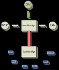
a microchip on some PC motherboards and is connected directly to the CPU (unlike the southbridge) and thus responsible for tasks that require the highest performance |
|
|
front-side bus (FSB)
|
a computer communication interface (bus) often used in Intel-chip-based computers during the 1990s and 2000s. The competing EV6 bus served the same function for AMD CPUs. Both typically carry data between the central processing unit (CPU) and a memory controller hub, known as the northbridge.
|
|
|
Intel QuickPath Interconnect (QPI)
|
a point-to-point
processor interconnect developed by Intel which replaced the front-side bus (FSB) in Xeon, Itanium, and certain desktop platforms starting in 2008 |
|
|
Direct Media Interface (DMI)
|
Intel's proprietary link between the northbridge and southbridge on a computer motherboard
- DMI shares many characteristics with PCI Express, using multiple lanes and differential signaling to form a point-to-point link. Most implementations use a ×4 link - first used between the 9xx chipsets and the ICH6, released in 2004 - DMI 2.0, introduced in 2011, doubles the transfer rate to 20 Gbit/s with a ×4 link. It is used to link an Intel CPU with the Intel Platform Controller Hub (PCH), which supersedes the historic northbridge/southbridge implementation - DMI 3.0, promising speeds of up to 8 GT/s, will be used by two-chip variants of the upcoming Intel Skylake microprocessors, which will be used in conjunction with Intel 100 Series chipsets; some variants of Skylake will have the PCH integrated into the die, effectively following the system on a chip (SoC) design layout |
|
|
HyperTransport (HT), formerly known as Lightning Data Transport (LDT)
|
is a technology for interconnection of computer processors. It is a bidirectional serial/parallel high-bandwidth, low-latency point-to-point linkthat was introduced on April 2, 2001
|
|
|
backside bus (BSB) |
-not always present -connects CPU with L2 & L3 (external cache) |
|
|
Southbridge |
-directly connected to the Northbridge -provides support for onboard slower peripherals (PS/2, parallel ports, serial ports, etc.) |
|
|
Peripheral Component Interconnect (PCI) |
-32-bit -operate at 33 or 66 MHz over a 32-bit(4-byte) channel -shared bus technology, cards will reduce to slowest speed - 3.3V notched toward the rear - 5V notched toward the front |
|
|
PCI-Extended (PCI-X) |
-a 64-bit computer bus and expansion card standard that enhances the 32-bit PCI local bus for higher bandwidth demanded mostly by servers andworkstations. It is a double-wide version of PCI, running at up to four times the clock speed, but is otherwise similar in electrical implementation and uses the same protocol
-shared bus technology, cards will reduce to slowest speed |
|
|
Accelerated Graphics Port (AGP) |
-designed to be a direct connection between the video circuitry and the PC's memory -32-bit channel 66 MHz clock -AGP 2x, 4x, and 8x multiple the 66 MHz speed |
|
|
PCI Express (PCIe) |
-a high-speed serial computer expansion bus standard designed to replace the older PCI, PCI-X, and AGP bus standards. PCIe has numerous improvements over the older standards, including higher maximum system bus throughput, lower I/O pin count and smaller physical footprint, better performance scaling for bus devices, a more detailed error detection and reporting mechanism (Advanced Error Reporting, AER[1]), and native hot-plugfunctionality -uses a switching component with point-to-point communication to the slots giving each card full bandwidth ( star topology) - 7 link widths x1, x2, x4, x8, x12, x16, x32; x1, x4, and x16 most common |
|
|
Scalable Link Interface (SLI)
|
is a brand name for a multi-GPU technology developed by NVIDIA for linking two or more video cards together to produce a single output. SLI is an algorithm of parallel processing for computer graphics, meant to increase the processing power available for graphics
|
|
|
AMD CrossFireX (previously known as CrossFire)
|
a brand name for the multi-GPU solution by Advanced Micro Devices, originally developed by ATI Technologies. The technology allows up to four GPUs to be used in a single computer to improve graphics performance
|
|
|
Communications and Networking Riser (CNR) |
-older technology used to remove analog I/O from the mother board |
|
|
pin grid array (PGA) |
pins are in a row/column orientation, an array of pins |
|
|
land grid array (LGA) |
a type of surface-mount packaging for integrated circuits (ICs) that is notable for having the pins on the socket rather than the integrated circuit. An LGA can be electrically connected to a printed circuit board (PCB) either by the use of a socket or by soldering directly to the board
|
|
|
socket 478 |
type: PGA-ZIF contacts: 478 FSB Protocol: AGTL+ Processors: Intel Pentium 4 (1.4 - 3.4 GHz) Intel Celeron (1.7 - 2.8 GHz) Celeron D (2.13 - 3.2 GHz) Intel Pentium 4 Extreme Edition (3.2, 3.4 GHz) |
|
|
socket 604 |
type: PGA contacts: 604 processor: Intel Xeon |
|
|
LGA 775 (Socket T) |
type: LGA contacts: 775 FSB Protocol: AGTL+ Processors: -Intel Pentium 4 (2.60 - 3.80 GHz) -Intel Celeron D (2.53 - 3.60 GHz) -Intel Pentium 4 Extreme Edition (3.20 - 3.73 GHz) -Intel Pentium D (2.66 - 3.60 GHz) -Pentium Extreme Edition (3.20 - 3.73 GHz) -Pentium Dual-Core (1.40 - 3.33 GHz) -Intel Core 2 Duo (1.60 - 3.33 GHz) -Intel Core 2 Extreme (2.66 - 3.20 GHz) -Intel Core 2 Quad (2.33 - 3.00 GHz) -Intel Xeon (1.86-3.40 GHz) -Intel Celeron (1.60 - 2.40 GHz) |
|
|
LGA 1156 (Socket H)
|
type: LGA contacts:1156 FSB Protocol: PCIe 16× (video) + 4× (DMI) + 2 DP (FDI), 2 DDR3 channels Processors: Intel Celeron Intel Pentium Intel Core i3 Intel Core i5 Intel Core i7 Intel Xeon |
|
|
LGA 1155 (Socket H2) |
type: LGA contacts 1155 processors: Sandy Bridge, Ivy Bridge |
|
|
LGA 1150 (Socket H3) |
type: LGA contacts: 1150 processors: Haswell, Broadwell |
|
|
LGA 1151 |
type: LGA
contacts: 1151 processors: Skylake |
|
|
LGA 1366 (Socket B) |
type: LGA contacts: 1366 FSB Protocol: QPI Processors Intel Core i7 (9xx series) Intel Xeon (35xx, 36xx,55xx, 56xx series) Intel Celeron P1053 |
|
|
LGA 1356 (Socket B2) |
type: LGA
contacts: 1356 FSB Protocol: QPI processors: Sandy Bridge |
|
|
LGA 2011( Socket R) |
type: LGA contacts: 2011 FSB Protocol: QPI, DMI 2.0 Processors Sandy Bridge-E/EP Ivy Bridge-E Haswell-E Haswell-EP |
|
|
LGA 1567 (SOCKET S) |
type: LGA contacts: 1567 FSB protocol: QPI Processorts: Xeon Beckton(Nehalem) Xeon E7 |
|
|
socket 940 |
TYPE: PGA-ZIF contacts: 940 Processors: AMD Athlon 64 FX AMD Opteron |
|
|
socket AM2 |
type: PGA-ZIF contacts: 940 Processors: Athlon 64 Athlon 64 X2 Athlon 64 FX Opteron Sempron Phenom |
|
|
socket AM2+ |
type: PGA-ZIF contacts: 940 Processors: Athlon 64 Athlon 64 X2 Athlon II Opteron Phenom series Phenom II series |
|
|
socket AM3 |
type: PGA-ZIF
contacts: 941 (Socket) 938 (CPU) Processors: Phenom II Athlon II Sempron Opteron 138x DDR3 capable CPUs |
|
|
socket AM3+ |
type: PGA-ZIF
contacts: 942(Socket) 938 (CPU) Processors: Phenom II Athlon IIFX -specified for CPU's based on the Bulldozer microarchitecture and designed to accept AM3 CPUs |
|
|
socket FM1 |
type: PGA-ZIF
contacts: 905 Processors: AMD Fusion APUs that incorporate CPUs and GPUs, such as E2-3200 and the A Series |
|
|
Complementary metal–oxide–semiconductor (CMOS)
|
memory chip that stores the system configuratioin |
|
|
dual in-line package (DIP)
|
an electronic component package with a rectangular housing and two parallel rows of electrical connecting pins
|
|
|
DIP switch
|
a manual electric switch that is packaged with others in a group in a standard dual in-line package (DIP)
|
|
|
firmware |
any software that is encoded in hardware |
|
|
Basic Input/Output System (BIOS)
|
a type of firmware used during the booting process (power-on startup) on IBM PC compatiblecomputers
|
|
|
Unified Extensible Firmware Interface (UEFI)
|
a specification that defines a software interface between an operating system and platform firmware. UEFI is meant to replace the Basic Input/Output System (BIOS) firmware interface, originally present in all IBM PC-compatible personal computers
|
|
|
power-on self-test (POST) |
a series of system checks performed by the system BIOS and other high-level components |
|
|
Hyper-Threading Technology or HTT
|
Intel's proprietary simultaneous multithreading (SMT) implementation used to improve parallelization of computations (doing multiple tasks at once) performed on x86 microprocessors
|
|
|
error-correcting code ECC |
if memory supports ECC, checks bits are generated and stored with the data, an algorithm is performed on the data and its check bits whenever the memory is accessed |
|
|
dynamic random access memory DRAM |
a type of random-access memory that stores each bit of data in a separate capacitor within an integrated circuit |
|
|
asynchronous DRAM ADRAM |
does not depend on the system clock |
|
|
Synchronous dynamic random access memory (SDRAM)
|
that is synchronized with the system bus. Classic DRAM has an asynchronous interface, which means that it responds as quickly as possible to changes in control inputs. SDRAM has a synchronous interface, meaning that it waits for aclock signal before responding to control inputs and is therefore synchronized with the computer's system bus
|
|
|
SDR SDRAM (Single Data Rate synchronous DRAM) |
transmits 1 bit of data per data pin every time the system clock ticks |
|
|
double data rate (DDR) SDRAM |
doubles the data rate of SDR SDRAM by reading/writing at the rising and falling of each clock cycle |
|
|
DDR2 SDRAM |
still uses the rise/fall of system clock like DDR, but internally DDR2 splits each clock pulse in half again higher latency |
|
|
DDR3 SDRAM |
splits the clock cycle again, similar to DDR2 |
|
|
DRDRAM - direct Rambus DRAM |
a type of synchronousdynamic RAM. RDRAM was developed by Rambus inc., in the mid-1990s as a replacement for then-prevalentDIMM SDRAM memory architecture
|
|
|
DIMM dual inline memory module |
-memory package -used both sides of the pins -SDR 84 pins each side, total of 168 independent pins -DDR 184 pins -DDR2 240 pins -DDR3 240 pins (incompatible with DDR2) |
|
|
RIMM Rambus inline memory module |
-used with DRDRAM -16-bit modules have 184 pins with 2 notches -32-bit modules have 232 pins with 1 notch |
|
|
SODIMM small outline DIMM |
-smaller form factor memory for laptops -all 64-bit variants have a single keying notch -144 pin SDR -200 pin DDR/DDR2 -204 pin DDR3 |
|
|
microDIMM |
-about 50% smaller than SODIMM (45.5 X 30 mm) -designed for sub-notebooks -144 pin for SDR -172 pins for DDR -214 pins for DDR2 |
|
|
Bulldozer (microarchitecture)
|
the codename for a microprocessor microarchitecture developed by AMD for the desktop and server markets. It was released on October 12, 2011 as the successor to the K10 microarchitecture.Bulldozer is designed from scratch, not a development of earlier processors. The core is specifically aimed at computing products with TDPs of 10 to 125 watts. AMD claims dramatic performance-per-watt efficiency improvements in high-performance computing (HPC) applications with Bulldozer cores.
|
|
|
Haswell (microarchitecture)
|
the codename for a processor microarchitecture developed by Intel as the successor to the Ivy Bridge microarchitecture; uses a 22 nm process
|
|
|
Broadwell (microarchitecture)
|
is Intel's codename for the 14 nanometer die shrink of its Haswell microarchitecture
H and C variants will be used in conjunction with Intel 9 Series chipsets (Z97, H97 and HM97), in addition to retaining backward compatibility with some of the Intel 8 Series chipsets |
|
|
Skylake (microarchitecture)
|
the codename used by Intel for a processor microarchitecture under development and due to launch in 2015 as the successor to the Broadwell microarchitecture
|
|
|
Ivy Bridge (microarchitecture)
|
the codename for a line of processors based on the 22 nm manufacturing process developed by Intel
22 nm die shrink of the Sandy Bridge microarchitecture |
|
|
Sandy Bridge (microarchitecture)
|
is the codename for a microarchitecture developed by Intel beginning in 2005 for central processing units in computers to replace the Nehalem microarchitecture.
|
|
|
Westmere (microarchitecture)
|
the name given to the 32 nm die shrink of Nehalem
|
|
|
Nehalem (microarchitecture)
|
the codename for an Intel processor microarchitecture, which is the successor to the older Core microarchitecture
use the 45 nm process, run at higher clock speeds, and are more energy-efficient than Penryn microprocessors. Hyper-threading is reintroduced, along with a reduction in L2 cache size, as well as an enlarged L3 cache that is shared among all cores. |